Single-crystalline antiferromagnetic layers
Antiferromagnetic (AFM) materials offer a lot of advantages over ferromagnetic (FM) materials: They are less susceptible against disturbing external magnetic fields, neighboring structures do not couple magnetostatically, they exhibit a much faster dynamics, and there is a greater choice of insulating antiferromagnetic materials than of ferromagnetic ones. Despite its technological importance for the development of advanced magnetic data storage devices and extensive studies, the details of the magnetic interface coupling between antiferromagnets and ferromagnets have remained concealed. This is in part due to the incomplete characterization of the interface in the sputtered polycrystalline samples that are typically used. Characterization and control of the interface structure and morphology at the atomic level is indeed the important issue, because the atomic spins in an antiferromagnet change their direction on the length scale of nearest atomic distances.
Example 1: Temperature-induced spin-state transition in NiMn
The magnetic coupling between two FM layers across an AFM spacer layer contains information about the spin structure of the antiferromagnet. The AFM spin structure directly affects the exchange coupling at the interface between the FM and the AFM material. We have observed a temperature-induced change of the spin state of a Ni0.4Mn0.6 layer sandwiched between perpendicularly magnetized FM Ni layers. The coupling between the Ni layers is deduced from minor-loop measurements by the magneto-optical Kerr effect (MOKE). The figure shows magnetization loops of a Ni/Ni0.4Mn0.6/Ni trilayer on Cu(001) with different AFM-layer thicknesses at temperatures as indicated.
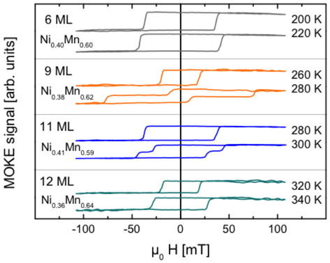
Above a certain transition temperature that depends on the thickness of the antiferromagnetic spacer layer, a strong magnetic coupling between the two Ni layers appears that is absent below that temperature. The direction of the coupling, parallel or antiparallel, depends on whether the antiferromagnetic NiMn layer consists of an even or odd number of atomic layers. The two-step loops in the figure show that for 9 and 11 atomic monolayers (ML) thickness, antiparallel coupling is observed at the higher of each of the two displayed temperatures. In contrast, for 6 and 12 ML thickness, the occurrence of parallel coupling manifests itself only by a jump of the coercivity with temperature. This result is interpreted as a transition of the antiferromagnetic spin structure of the NiMn layer that strongly affects the interlayer exchange coupling of the two ferromagnetic layers by direct exchange through the antiferromagnetic layer. Such a transition is also highly interesting for utilizing in dynamic processes, since the effect of a relatively small transient raise of temperature is enhanced by the strong and nonlinear increase in interface coupling.
Example 2: Atomic-scale spin structure of ultra-thin Mn films
The interaction of an AFM material with its surrounding is governed by the antiferromagnetic spin structure. Since the atomic moments cancel on the length scale of atomic distances, high-resolution microscopy is required for the direct determination of the AFM spin structure. We used high-resolution spin-polarized scanning tunneling microscopy (STM) at room temperature with a bulk iron ring as spin-polarized scanning probe to image the spin structure at the surface of an epitaxial Mn film, grown on Co/Cu(001).
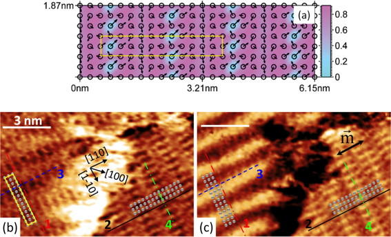
The figure shows in panel (b) the topographic STM contrast, revealing a (12 × 2) geometric reconstruction of the Mn surface with two domains, rotated by 90° with respect to each other. The white dots indicate single-atomic distances in the surface, the yellow rectangle shows the size of the superstructure unit cell. Panel (c) displays a differential conductance map at +0.2 V bias voltage at the same sample position. The black double-headed arrow points out the orientation of the Fe ring probe, which breaks the symmetry of the two orthogonal domains. The different appearance of the two domains in (c) evidences the influence of spin-polarized electron tunneling. A noncollinear spin structure that is consistent with the experimental data is shown in (a), where the arrows show the in-plane component of the individual atomic spins, while colors indicate the absolute value of the out-of-plane component, as defined in the legend on the right-hand side. We attribute the noncollinear spin structure of Mn to competing antiferromagnetic exchange interactions in the frustrated and reconstructed Mn layer.
Example 3: Competition for exchange-bias pinning in Ni/Ni25Mn75/Ni trilayers
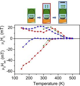
The behavior of the exchange bias effect, the unidirectional magnetic coupling of a ferromagnetic layer by an AFM layer, in the presence of a second ferromagnetic layer at the other interface of the AFM layer can yield important information about the nature of the pinning of spins in the AFM layer. We have studied (Co/)Ni/Ni25Mn75/Ni(/Co) trilayers, epitaxially grown on a Cu3Au(001) substrate. The optional Co layers were used to change the magnetization direction of the Ni films from perpendicular to the film plane into the film plane. The exchange bias (bottom part of the graph) of the bottom Ni/Co ferromagnetic film with in-plane magnetization (green curve) nearly does not change upon the deposition of a Ni layer with out-of-plane magnetization on top of the AFM Ni25Mn75 layer (red curve), but shrinks drastically once the magnetization direction of the top Ni layer is turned into the plane by a Co overlayer (blue curve). We interpret this in a model of competing non-collinear pinning centers throughout the entire thickness of the AFM Ni25Mn75 layer.
Publications about this research:
T. Hagelschuer, Y. A. Shokr, and W. Kuch
Spin-state transition in antiferromagnetic Ni0.4Mn0.6 films in Ni/NiMn/Ni trilayers on Cu(001)
Phys. Rev. B 93, 054428 (2016).
DOI: 10.1103/PhysRevB.93.054428
J. Song, C.-B. Wu, B. Zhang, J. Xu, and W. Kuch
Layer-dependent properties and noncollinear spin structure of epitaxial antiferromagnetic Mn films on Co/Cu(001)
Phys. Rev. B 91, 214406 (2015).
DOI: 10.1103/PhysRevB.91.214406
M. Y. Khan, C.-B. Wu, and W. Kuch
Pinned magnetic moments in exchange bias: Role of the antiferromagnetic bulk spin structure
Phys. Rev. B 89, 094427 (2014).
DOI: 10.1103/PhysRevB.89.094427
M. Y. Khan, Y. A. Shokr, and W. Kuch
Coupling of pinned magnetic moments in an antiferromagnet to a ferromagnet and its role for exchange bias
J. Phys.: Condens. Matter 32, 075801 (2020).
DOI: 10.1088/1361-648X/ab531a
J. Song and W. Kuch
The Growth and Crystalline Structure of Ultrathin Mn Films on Ni(111)
Phys. Stat. Sol. B 255, 1800173 (2018).
DOI: 10.1002/pssb.201800173