Equipment and techniques
Nanofabrication
To fabricate nanoscale devices, we operate a cleanroom facility at FU Berlin (SupraFab, Altensteinstraße 23a)). It currently includes the following tools:
- Electron beam lithography system (Raith Pioneer 2)
- Focussed ion beam system (FEIScios 2 Dual Beam)
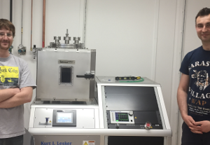
- Metal evaporator (KJLC Nano 36)
- Atomic Force Microscope (JPK Nanowizard)
- Optical microscopes with transfer stages for 2D materials (Nikon Eclipse LV-100)
- Plasma etchers (Diner Pico & Plasmatech MiniFlecto)
- Reactive Ionetching (Oxford RIE 80)
- Plasma enhanced vapor deposition (Oxford PECVD 80)
- GloveBox (Inert) with Transferstage (Graphene Industries), ezAFM (Nanomagnetic Instruments) and Molecular Evaporator (Angstrom Covap)
- Optical Lithographie tools (Heidelberg µMLA)
- Raman Spectrometer (Horiba Xplora)
Additionally we have in our Labs at Arnimallee 14 following devices for nanofabrication
- Wire Bonder (TPT HB05)
- Chemical vapor deposition (CVD) furnace for growth of 2D materials (homebuilt)
- Critical point dryer
Measurements
For electrical, optoelectronic, and mechanical measurements we have the following toys:
- Cryogenics Ltd. 1.5K, 12 Tesla cryostat
- Lakeshore low temperature probestation
- Custom scanning photocurrent setup
- Custom cryostat with nanomechanical manipulation and optical access
- Low temperature photoluminescence/Raman setup with gas access