Research projects
|
|
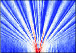
Quantum transport at ultrahigh carrier densities in 2D materialsCharge carriers (electrons and holes) change their character in 2D materials. In graphene, for example, the charge carriers behave as relativistic massless particles obeying the Dirac equation. In high magnetic fields and at low temperatures, they form fractionally charged quasiparticles. In monolayer transition metal dichalcogenides (TMDs), photoexcited electron/hole pairs bind into “excitons” that have properties similar to that of Hydrogen atoms. However, the most interesting and currently unstudied “corner” of the phase diagram of 2D materials is the regime of high carrier densities and high electrical fields. Graphene, for example, is predicted to become a superconductor with near-room transition temperature at very high doping. Monolayer TMDs at high applied fields may undergo a phase transition and become an excitonic insulator. The goal of this project is to achieve ultra-high electrical fields and doping densities in 2D materials and to study quantum transport in this regime. To accomplish this, we develop a new technology to apply ultra-large fields to 2D materials using advanced ionic gating. |
|
|
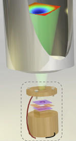
Nanomechanics and strain engineering of 2D membranesMechanical stretching and bending dramatically changes the properties of 2D materials. First, electrons in non-uniformly strained graphene are expected to behave exactly as if they were exposed to strong out-of-plane magnetic field. This “pseudomagnetic field” should even lead to the emergence of a Quantum Hall-like quantization. Similar pseudo-magnetic field was predicted to act on pseudospin degree of freedom in strained monolayer TMDs. Second, the applied mechanical strain drives direct-to-indirect bandage transition, changes the topology of the Fermi surface, and may even lead to topological phase transitions. Third, mechanical strain changes the spectrum of flexural (out-of-plane) phonons of 2D materials. This phonon branch unique to thin membranes has divergent density of states, quadratic dispersion and zero group velocity. Flexural phonons make mechanical properties of 2D materials are closer to that of biological membrane than conventional solids: the thermal expansion coefficient of 2D materials is negative, stiffness is a non-linear function of strain, the Poison ratio is negative. The applied mechanical strain suppresses flexural phonons and changes every mechanical parameter. The goal of this project is to unlock predicted but experimentally unobserved phases and to controllably modify the Hamiltonians of 2D materials by mechanically stretching and bending them. To accomplish this, we develop tools and technique to apply mechanical strain to nanoscopic monolayer materials in vacuum and at low temperatures. |
|
|
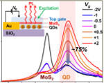
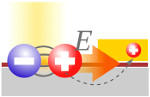
Two-dimensional excitons talking to their environmentMonolayer TMDs (e.g. monolayer molybdenum disulfide) are semiconducting 2D materials with direct bandgap in the visible range. An electrostatically bound electron-hole pair called an exciton is created in TMDs following photon absorption. Excitons are condensed-matter analogs of Hydrogen atoms and feature all of the phenomena familiar from the atomic physics — excited states, fine structure, Stark effect, etc… At the same time, excitons in monolayer TMDs are two-dimensional and strongly interact with the environment around them. In this project, we explore these interactions both to understand the fundamental physics of low-dimensional excitons and to develop technologies for potential applications. For example, we have shown that excitons in TMDs are strongly screened by their environment, that different excitons “feel” the dielectric function of the environment at different frequencies depending on exciton symmetries, and that nanoscale light emitters, such as quantum dots (QDs) effectively exchange energy with excitons via near-field processes. Moreover, we showed the emission of light by QDs proximally coupled to a TMD can be switched “on” and “off” by electrostic gating the TMD. This phenomenon may be useful in display technology. Currently, we are studying complex excitonic states formed between TMDs and atoms or molecules deposited on their surface. |
|
|
Probing excitons, spin, pseudospin in 2D materials via photocurrent spectroscopyMonolayer TMDs are interesting for applications in spintronics. The presence of two distinct valleys in their bandstructure leads to the appearance of an additional valley or “pseudospin” degree of freedom. The non-centrosymmetric crystal structure causes a “locking” between spin and valley degrees of freedom, thereby increasing the spin lifetime and allowing spin-selective optical excitation. The overarching goal of this project is to study the ultrafast transport of spins in monolayer TMDs. Using a combination of ultrafast Kerr rotation microscopy (trKR) and time-resolved photocurrent spectroscopy (trPC), we will study coupled ultrafast dynamics of charge, spin, pseudospin, and excitons inTMDCs and TMDC/metal interfaces. We will answer the following questions: How fast do photoexcited spins, charges, and excitons in TMDCs travel and relax and what factors affect their relaxation dynamics? What effects (e.g. induced spin/orbit coupling, exchange fields, induced magnetism) arise in TMDCs in the proximity of ferromagnets and which processes govern the charge and spin transfer across a TMDC/metal interface? How do “pseudomagnetic fields”arising in strained TMDCs affect spin dynamics? In a long run, we intend to explore the potential of TMDCs towards applications in ultrafast spintronic devices and to achieve the ultrafast control of the ferromagnetic phase in TMDCs. |
|
|
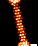
In-situ microscopy and modification of 2D materialsEvery atom in 2D materials is on the surface and can be directly visualized via high-resolution microscopy techniques such as Scanning Transmission Electro Microscopy (STEM). The goal of this project is to visualize, in real time, changes in the atomic structures of 2D materials under the influence of external factors -- strong electrical field, temperature, current flow. We are especially interesting in understanding and visualizing the process of intercalation — the “insertion” of foreign atoms between the layers of multi-layered of 2D materials. Chemical intercalation is the basis of battery technology and its understanding may be important in improving the performance of existing batteries. To carry out this project, we develop technique to visualize the atomic structures of intercalated materials as this process occurs. The project is a collaboration with the STEM group at the Oak Ridge National Laboratory (US). |